For decades, Si has dominated the semiconductor market due to its abundance and low cost. Almost every circuit has some Si based component. Power Electronic circuits are no exception. To this date, most converters use Si transistors as switches. More than 60% of the space on a converter circuit board is occupied by bulk capacitors and magnetic components. Because these components transfer energy every second, their size depends on the operating frequency. Si fails to provide considerable size reduction in high power circuits because it struggles to operate efficiently at high frequencies (>100kHz). Hence, Si-based high-power solutions tend to be bulky. This is where GaN steps in
GaN enables efficient operation at high frequencies (>100kHz) which means that the
size of magnetic
components can be decreased allowing for power efficient high-power density
circuits. GaN based
converters are more compact, dissipate lesser heat and pack more power per unit
volume than their
Si-counterparts. The BLDC driver under development at IIT-B uses GaN transistors to
operate at higher
frequency because at high frequencies, the current ripple and hence the amount of
DC-Link capacitance
required decreases. This means that smaller film capacitors can be used instead of
bulky electrolytic
capacitors. With GaN transistors, the team was able to increase the operating
frequency to 4x that of initial
prototype and get 50% theoretical reduction in C-Link capacitance and 40% lesser
losses per switch.
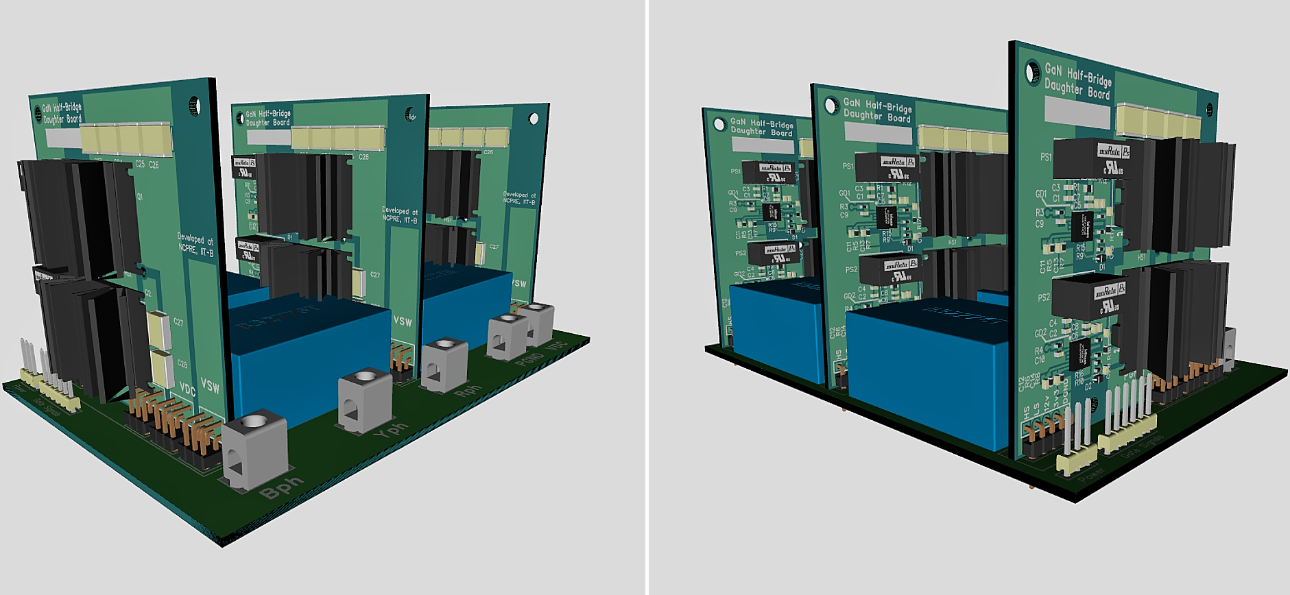
Owing to higher operating frequency, lesser losses and easier thermal management,
the team was able to
decrease the power stage size to 1/3rd that of the Si-based prototype. This allowed
them to design
modular half bridge cards (daughter boards). 3 such daughter boards when plugged
into a motherboard
(which carries DC-Link capacitors) complete the power stage of the BLDC driver. This
plug-n-play features
makes the motor driver highly modular. In case of a failure in any of the phases,
the corresponding
daughter board can be simply pulled out and replaced like a Lego block. This
modularity facilitates easy
debugging, quicker maintenance and shorter downtime.
| Criteria | Si | GaN | Reason |
|---|---|---|---|
| Operating Temp | Lower | Higher | GaN has higher Bandgap than Si |
| Operating Temp | Lower | Higher | GaN device has lower CISS, COSS meaning faster turn-on, turn-off and lower switching losses |
| Device Size | Bigger | Smaller | GaN has higher critical elec. field, which means for same breakdown voltage, GaN device can be much smaller (VBR = 0.5*wdriti*Ecrit) |
| RDS-ON | Lower | Higher | Higher electron density and much smaller drift region in GaN |
| Device Parasitic | Lower | Higher | Instead of Au bond wires, modern GaN devices have a “laminated structure” interconnected with thick Cu-filled vias for terminal connections |
| Cost | Lower | Higher | Fabrication Complexity |