
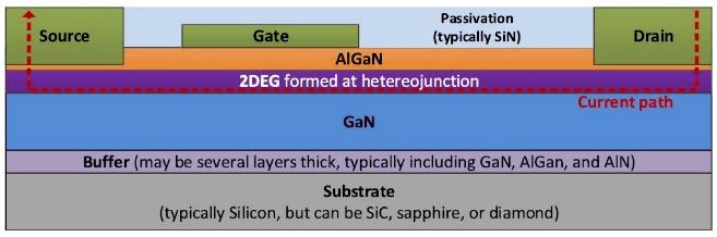
High band gap based GaN HEMT devices are gaining the interest of the industry due to their very fast switching action and very low Figure of Merit in comparison to their Si counterparts. The hetero-junction structure and characteristics of the GaN devices lead to a very different behaviour compared to Si MOSFETs. The ultra-small parasitic capacitance makes it possible to deplete the two-dimensional electron gas (2DEG), the layer responsible for current conduction, even before the switching-off transition. This results in an extremely low switching loss during the turn-off action of the switch.
The synchronous boost converter schematic, shown in figure, is fabricated using GaN HEMTs, which is operated at a frequency of 1 MHz. This leads to smaller size of the inductors and capacitors required. In addition, the losses in GaN devices are almost 3 to 5 times lower than similar rated Si devices. Due to the small size of passive elements, and GaN devices in general having small footprint due to their high breakdown strength, it is possible to design very compact and highly efficient converters.
We have designed a synchronous boost converter which is compact (about one third of regular size converter) while achieving high conversion efficiency. Based on the simulation results, an efficiency of 97.8% is obtained for a synchronous boost converter supplying a load of 5kW (neglecting losses in auxilliary circuits).
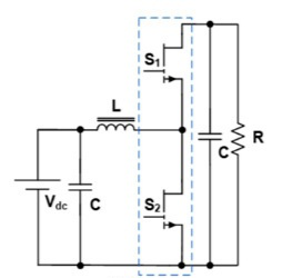 Half-bridge-based Synchronous Boost converter
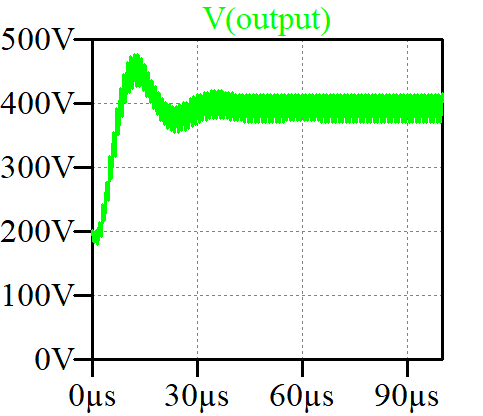 Output Voltage
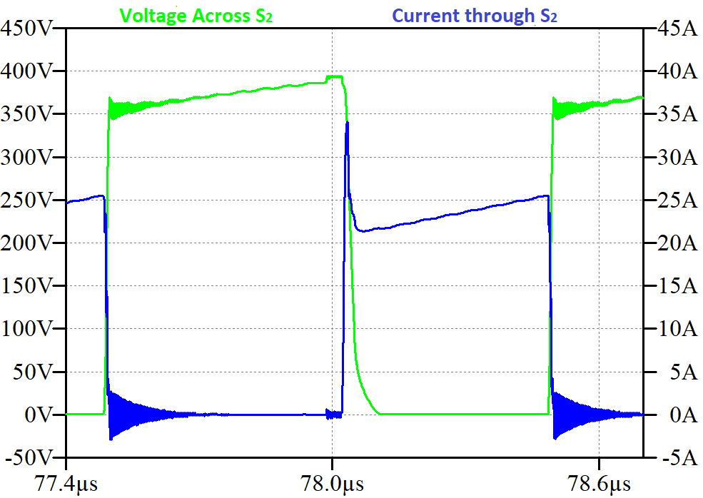 Switching voltage and Current.